Introduction
Interfacing a 16X2 or 16X4 LCD module with a 3.3V MCU is not same as interfacing with MCUs like AVR which operate on 5Volts. As per request by some of the readers of previous articles on lpc2148 this article is on Interfacing a 5V LCD Module with LPC2148 MCU and in general for any ARM or 3.3V MCU .
Whats next? : A simple Library for LCD interfacing with LPC214x and LPC176x MCUs. And more tutorials on Timer , PWM , UART .. for lpc214x , lpc176x.
For this article I’ve used the readily available Chinese 16X2 LCD Module : JHD-162A. The Data sheet for JHD-162A 16X2 LCD Module is located at : http://www.egochina.net.cn/eBay/Download/JHD162A.pdf I would strongly suggest that you keep that datasheet open when reading this article to avoid any sort of confusion.
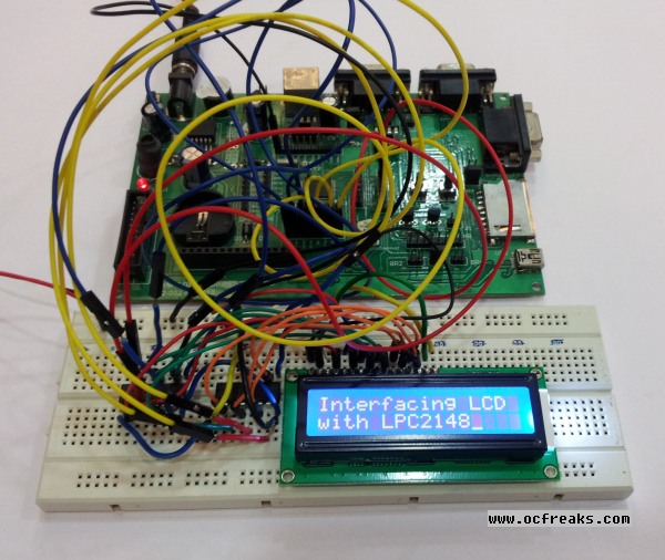
Before Starting the Tutorial , as a motivation , I would like to show the final outcome of this tutorial. The pic below shows the LPC2148 development board interfaced with JHD162A LCD Module via 2x HCF4050B ICs. I’ll come to HCF4050B IC shortly .. at the moment lets get started with the basics.
16X2 LCD Basics :
This particular chinese LCD i.e JHD162A has KS0066U controller or similar to the famous HD44780U. It Consists of 2 Rows with 16 Characters on each. It has a 16 pin Interface. Operates on 5V and has LED backlight. Works in 2 Modes :
- 1) Instruction Mode : Used for initializing and configuring LCD before we can use it & during operation.
- 2) Data Mode : Displays the respective characters for codes supplied to it via Data Pins.
Standard Pinout is as follows :

To keep things simple lets group the pins into 3 :
1) Power Pins : Pin 1,2,3,15,16
2) Control Pins : Pin 4,5,6
3) Data Pins : Pin 7 to 14
- Contrast Voltage (VEE) : Instead of using a trim pot just connect a 1K resistor to VEE in series and ground it. That gives the best contrast of what I’ve seen.
- RS – short for Register select (Control Pin) : Used to switch been Instruction and Data Mode. RS = High for Instruction Mode and RS = Low for Data mode.
- R/W – Read or Write (Control Pin): R/W = High for Read Mode and R/W = Low for Write. Since we are going to use Write Mode only we will permanently ground it using a pull-down resistor of 4.7K Ohms. Caution : If you are planning to use Read Mode with 3.3V MCUs you’ll need a Bi-directional level shifter which can shift 5V to 3.3V and Vice-Versa.
- Enable (Control Pin) : This is similar to a trigger pin. Each Data/Instruction is executed by the LCD module only when a pulse is applied to Enable pin. More specifically the it is executed at the falling edge of the pulse.
If you want to know the fundamentals and internal operation of LCD Modules I would recommend visiting these links :
- http://lcd-linux.sourceforge.net/pdfdocs/lcd1.pdf
- http://lcd-linux.sourceforge.net/pdfdocs/lcd2.pdf
- http://www.8051projects.net/lcd-interfacing/ (Covers a lot of basics .. I found it really helpful.)
Interfacing 5V LCD Module with lpc214x:
5V LCD wont operate on 3.3V and also since lpc214x runs on 3.3V and 5Volts might fuse some of its GPIO pin we are gonna need a level shifter or translator that can shift 3.3Volts to 5Volts for LCD Module to be safe. Vikram Sharma M. has successfully interfaced JHD162A with MSP430 MCU using CD4050B IC as explained in his post @ http://msharmavikram.wordpress.com/2012/08/14/3-mistakes-of-lcd-with-msp430-solved/ .
Some of the buffers / level shifters than can be used are : SN74AHC244N , SN74AC241N , CD74AC244E , CD4050B , etc.. out of which CD4050B is readily available. I purchased a few HCF4050 which is same as CD4050B except it is manufactured by ST Microelectronics and not Texas Instruments.
HCF4050B is a non-inverting Hex Buffer. In our case we’ll be needing 2 of them at minimum since we are going to use 8+2=10 pins from MCU which need to be shifted to 5Volts. There are going to be 8 Data pins and 2 control pins connected from MCU to the LCD Module using 2x HCF4050B.
Connections from lpc214x to LCD module will be as shown below. I’ve also made a PCB for the schematic if bread-board is not your cup of tea.(Frankly , since I was running out of time I did it using a bread-board. If some one is having any problems with PCB please let me know.)
1)Pin Connections from MCU to HCF4050B ICs :
IC1 : P1.16->Pin3 , P1.17->Pin5 , P0.0->Pin7 , P0.1->Pin9 , P0.2->Pin11 , P0.3->Pin14
IC2 : P0.4->Pin3 , P0.5->Pin5 , P0.6->Pin7 , P0.7->Pin9 (Pins 11,14 of IC2 are NC)
2)Pin Connections from HCF4050B to LCD Module :
IC1 : Pin2->RS , Pin4->Enable , Pin6->DB0 , Pin10->DB1 , Pin12->DB2 , Pin15->DB3
IC2 : Pin2->DB4 , Pin4->DB5 , Pin6->DB6 , Pin10->DB7 (Pin 12,15 of IC2 are NC)

Download links to PCB pdf and Eagle 6.2+ (Schematic+Board) Design Files:
1) lcd_interface_arm_mcu_PCB-pdf.rar
2) lcd_interface_arm_mcu-EAGLE-6.2+design-files.rar
Components required at bare minimum :
- LPC214x Development board
- 16X2 LCD Module
- 2x HFC4050B or CD4050B
- 5V Supply for LCD
- Resistors : 1x 1K , 1x 4.4K , 1x 47 Ohms
- Bread-Board / Self-made PCB
- Berg Strips , Jumper wires
Initializing LCD Module :
After you have cross-checked all your connections from MCU to HFC4050 to LCD Module its time now to Display text on LCD. But before that we need to initialize the LCD properly. Also NOTE that : as per the Datasheet – before initializing LCD we need to wait for a minimum time of about 15ms after the input voltage supply is stable and >4.5Volts.
The 1st thing required for this is that RS must be held LOW and Enable also LOW in the beginning. Now we must supply some commands using the Data Pins to LCD. But this command wont be executed until we supply a pulse to Enable Pin. After supplying the command we make enable High and then Low after a short delay(i.e a Pulse) and the command is executed.
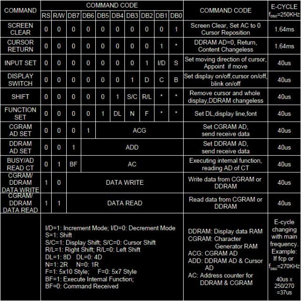
Codes for various instructions can be obtained from below table : (Refer to page 12 of the Datasheet)
- Function Set
- Display Switch
- Input Set
- Screen Clear Command
- DDRAM AD Set – Resposition Cursor Command
- In our case we are going to use 8Bit Mode with 2Rows and 5×10 Font style which gives Function set as 0x3C.
- Next we issue Display On , Cursor On , Blink On which gives Display Switch as 0x0F.
- Next we select Increment Mode which gives Input Set as 0x06.
- Now we clear the screen and set cursor at Home which gives Screen Clear as 0x01.
- Also the command to reposition the cursor at Home at anytime is 0x80 and to reposition it at the 1st column of the second row is 0xC0.
To cut-short or in simple words: We need to supply 5 commands in given order to the Data Pins with a small amount of delay in between to initialize the LCD properly. These commands are : 0x3C , 0x0F , 0x06 , 0x01 , 0x80(actually not required). Now since we have used the the 1st eight pins of port 0 on lpc214x we can directly assign these values to the IO0PIN register. Note that Bit 0 i.e LSB in IO0PIN is towards extreme right and the bit number increases as we move towards the left approaching the MSB. Also since we have connected P0.0 to Data Bit 0 pin , P0.1 to Data bit 1 and so on … we have a one to one consecutive mapping between them MCU pins and LCD Data pins.
Correct Sequence for Initializing LCD module (8 Bit Interface) is as given :
- After LCD Module is powered on and MCU boots wait for 20ms (Specifically >15ms)
- Now make RS and Enable LOW making sure that R/W is permanently grounded.
- Issue Function set command – 0x3C and Pulse Enable (wait for >40us after pulsing).
- Issue Display Switch – 0x0F and Pulse Enable (wait for >40us after pulsing).
- Issue Input Set – 0x06 and Pulse Enable (wait for >40us after pulsing).
- Issue Screen Clear – 0x01 and Pulse Enable (wait for >1.64ms after pulsing).
- Issue DDRAM AD Set – 0x80 and Pulse Enable (wait for >40us after pulsing).
Now LCD is ready for Printing!
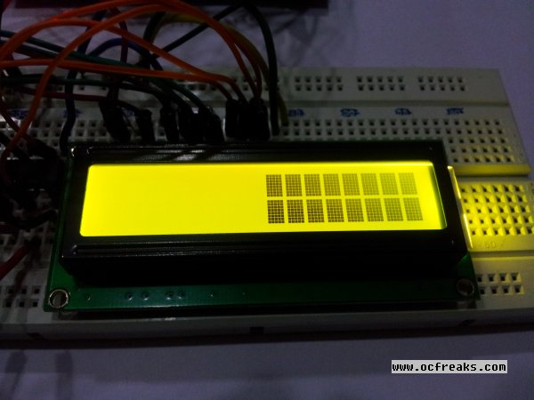
After Initializing the LCD you would see a Cursor Blinking at in 1st column at row 1 :
Printing Characters on LCD Module :
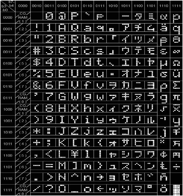
Now that we have initialized LCD correctly its time to send some characters. For this we enter into Data Mode by making RS High. After that any number / code applied to Data pins will be converted into corresponding Character and displayed. The codes for the characters are ASCII Codes given by the font table as show below :
Hence to print a character on LCD we just need to apply the 8bit ASCII code to Data pins. This can be done easily by type casting the character into an integer (which is done automatically by the compiler – but we are doing it here explicitly). Refer to Page 14 of datasheet for font table.
Now , after printing 16 characters you might wanna print more characters in 2nd Row. This is done by entering into Instruction Mode by holding RS=LOW and giving command 0xC0 which repositions the cursor at 2nd Row & 1st column. Needless to say that we need to again give a Pulse on Enable pin to process it. After that we put RS to high and get back in Data mode.
More on DDRAM and CGROM @ http://www.8051projects.net/lcd-interfacing/basics.php
Programs for Lpc2148 to print Characters on LCD module :
1st Let me explain a few functions that I’ve made in the programs below:
- initLCD() : Initializes the LCD.
- enable() : To generate a pulse on Enable pin.
- LCD_Cmd(int) : To issue LCD commands.
- LCD_WriteChar(char) : Print a Single Character.
- LCD_WriteString(string) : Print a String.
- delay() :Generate required delay.(For program1 Only!)
- delayMS(int) : Generate specificed delay.(For program2 Only!)
Program #1 : Basic Program without precise Timing & no PLL setup.
/*
 (C) OCFreaks! | Umang Gajera 2012-13.
 More Embedded tutorials @ www.ocfreaks.com/cat/embedded
 >>Program for Interfacing 16X2 LCD Module with LPC2148
*/

#include <lpc214x.h>

/*
 Connections from LPC2148 to LCD Module:
 P0.0 to P0.7 used as Data bits.
 P1.16 connected to pin4 i.e. RS	- Command / Data
 P1.17 connected to pin6 i.e. E - Enable
 Pin5 of LCD Module i.e. 'R/W' connected to ground
*/

void initLCD(void);
void enable(void);
void LCD_WriteChar(char c);
void LCD_WriteString(char * string);
void LCD_Cmd(unsigned int cmd);
void delay(void);


int main(void)
{
	initLCD(); //LCD Now intialized and ready to Print!
	LCD_WriteString(".: Welcome to :.");
	LCD_Cmd(0x80 + 0x40); //Come to 2nd Row
	LCD_WriteString("www.OCFreaks.com");
	while(1); // Loop forever
	return 0; //This won't execute :P
}

void initLCD(void)
{
	IO0DIR = 0xFF; //P0.0 to P0.7 configured as Output - Using 8 Bit mode
	IO1DIR |= (1<<16) | (1<<17); //P1.16 and P1.17 configured as Output - Control Pins
	IO0PIN = 0x0; //Reset Port0 to 0.
	IO1PIN = 0x0; //Reset Port1 to 0 - Which also makes RS and Enable LOW.

	//LCD Initialization Sequence Now starts
	delay(); //Initial Delay
	LCD_Cmd(0x3C); //Function Set Command : 8 Bit Mode , 2 Rows , 5x10 Font Style
	LCD_Cmd(0x0F); //Display Switch Command : Display on , Cursor on , Blink on
	LCD_Cmd(0x06); //Input Set : Increment Mode
	LCD_Cmd(0x01); //Screen Clear Command , Cursor at Home
	LCD_Cmd(0x80); //Not required the 1st time but needed to reposition the cursor at home after Clearing Screen
	//Done!
}

void enable(void)
{
	delay();
	IO1PIN |=  (1<<17);//Enable=High
	delay();
	IO1PIN &= ~(1<<17);//Enable=Low
	delay();
}

void LCD_WriteChar(char c)
{
	IO1PIN |= (1<<16); //Switch to Data Mode
	IO0PIN = (int) c; //Supply Character Code
	enable(); //Pulse Enable to process it
}

void LCD_WriteString(char * string)
{
	int c=0;
	while (string[c]!='\0')
	{
		LCD_WriteChar(string[c]);
		c++;
	}
}

void LCD_Cmd(unsigned int cmd)
{
	IO1PIN = 0x0; //Enter Instruction Mode
	IO0PIN = cmd; //Supply Instruction/Command Code
	enable(); //Pulse Enable to process it
}

void delay(void)
{
	int i=0,x=0;
	for(i=0; i<19999; i++){ x++; }
}
Program #2 : Program with PLL* setup and precise Timing**. (Xtal=12Mhz , CCLK=60Mhz)
*PLL tutorial for LPC2148 @ https://www.ocfreaks.com/lpc214x-pll-tutorial-for-cpu-and-peripheral-clock/
**Tutorial on Timer for LPC2148 @ https://www.ocfreaks.com/lpc2148-timer-tutorial/
/*
 (C) OCFreaks! | Umang Gajera 2012-13.
 More Embedded tutorials @ www.ocfreaks.com/cat/embedded
 >>Program2 for Interfacing 16X2 LCD Module with LPC2148
 >>using Timer0 and CPU @ 60Mhz
*/


#include <lpc214x.h>

/*
 XTAL Freq=12 Mhz , CCLK=60Mhz , PCLK=60Mhz
 Using common delay of 2ms for all operations

 Connections from LPC2148 to LCD Module:
 P0.0 to P0.7 used as Data bits.
 P1.16 connected to pin4 i.e. RS    - Command / Data
 P1.17 connected to pin6 i.e. E - Enable
 Pin5 of LCD Module i.e. 'R/W' connected to ground
*/

#define PLOCK 0x00000400

void initLCD(void);
void enable(void);
void LCD_WriteChar(char c);
void LCD_WriteString(char * string);
void LCD_Cmd(unsigned int cmd);
void delayMS(unsigned int milliseconds);

void setupPLL0(void);
void feedSeq(void);
void connectPLL0(void);


int main(void)
{
    setupPLL0();
    feedSeq(); //sequence for locking PLL to desired freq.
    connectPLL0();
    feedSeq(); //sequence for connecting the PLL as system clock

    //SysClock is now ticking @ 60Mhz!

    VPBDIV = 0x01; // PCLK is same as CCLK i.e 60Mhz

	//PLL0 Now configured!

	initLCD(); //LCD Now intialized and ready to Print!
    LCD_WriteString(".: Welcome to :.");
    LCD_Cmd(0x80 + 0x40); //Come to 2nd Row
    LCD_WriteString("www.OCFreaks.com");
    while(1); // Loop forever
    return 0; //This won't execute :P
}

void initLCD(void)
{
    IO0DIR = 0xFF; //P0.0 to P0.7 configured as Output - Using 8 Bit mode
    IO1DIR |= (1<<16) | (1<<17); //P1.16 and P1.17 configured as Output - Control Pins
    IO0PIN = 0x0; //Reset Port0 to 0.
    IO1PIN = 0x0; //Reset Port1 to 0 - Which also makes RS and Enable LOW.

    //LCD Initialization Sequence Now starts
    delayMS(20); //Initial Delay
    LCD_Cmd(0x3C); //Function Set Command : 8 Bit Mode , 2 Rows , 5x10 Font Style
    LCD_Cmd(0x0F); //Display Switch Command : Display on , Cursor on , Blink on
    LCD_Cmd(0x06); //Input Set : Increment Mode
    LCD_Cmd(0x01); //Screen Clear Command , Cursor at Home
    LCD_Cmd(0x80); //Not required the 1st time but needed to reposition the cursor at home after Clearing Screen
    //Done!
}

void enable(void)
{
    //Using common delay of 2ms
	delayMS(2);
    IO1PIN |=  (1<<17);//Enable=High
    delayMS(2);
    IO1PIN &= ~(1<<17);//Enable=Low
    delayMS(2);
}

void LCD_WriteChar(char c)
{
    IO1PIN |= (1<<16); //Switch to Data Mode
    IO0PIN = (int) c; //Supply Character Code
    enable(); //Pulse Enable to process it
}

void LCD_WriteString(char * string)
{
    int c=0;
    while (string[c]!='\0')
    {
        LCD_WriteChar(string[c]);
        c++;
    }
}

void LCD_Cmd(unsigned int cmd)
{
    IO1PIN = 0x0; //Enter Instruction Mode
    IO0PIN = cmd; //Supply Instruction/Command Code
    enable(); //Pulse Enable to process it
}

void delayMS(unsigned int milliseconds)
{
//Timers will be explained in detail in the very next tutorial @ www.ocfreaks.com/cat/embedded/

	T0IR = 0;
	T0CTCR = 0;
	T0PR = 60000; //60000 clock cycles @60Mhz = 1 mS
	T0PC = 0;
	T0TC = 0;
	T0TCR = 0x01; //enable timer

	//wait until timer counter reaches the desired dela1y
	while(T0TC < milliseconds);

	T0TCR = 0x00; //disable timer
}

//---------PLL Related Functions :---------------

void setupPLL0(void)
{
    PLL0CON = 0x01; // PPLE=1 & PPLC=0 so it will be enabled
                    // but not connected after FEED sequence
    PLL0CFG = 0x24; // set the multipler to 5 (i.e actually 4)
                    // i.e 12x5 = 60 Mhz (M - 1 = 4)!!!
                    // Set P=2 since we want FCCO in range!!!
                    // So , Assign PSEL =01 in PLL0CFG as per the table.
}

void feedSeq(void)
{
    PLL0FEED = 0xAA;
    PLL0FEED = 0x55;
}

void connectPLL0(void)
{
    // check whether PLL has locked on to the  desired freq by reading the lock bit
    // in the PPL0STAT register

    while( !( PLL0STAT & PLOCK ));

    // now enable(again) and connect
    PLL0CON = 0x03;
}
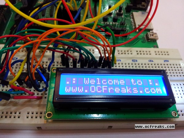
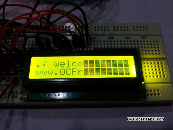
Output after flashing any of the above code to MCU (Successfully Tested on Lpc2148 and Lpc1768) :
Download Links to Source Code using KEIL UV4 Project IDE :
1) Program #1 : OCFreaks.com_LPC2148_LCD_Interfacing.rar
2) Program #2 : OCFreaks.com_LPC2148_LCD_Interfacing_precise.rar
Silence please : 2 LCDs were Harmed in the making
While working on this article 2 of my Green LCDs were damaged. One got completely useless and other got partially damaged. In any case both of them are useless now.
LCD #1 : Display completely gone kaput..
LCD #2 : Display partially gone kaput..

