Many ARM Cortex-M series of MCUs from NXP from the LPC1000 family viz. LPC11xx, LPC13xx, etc. have I/O configuration registers for Port Pins called IOCON. In this tutorial we will discuss about the structure of these register and how to use them when programming in C/C++. The structure of IOCON might vary depending on the specific micro-controller.
Each pin on MCUs like LPC1114, LPC1115, LPC1343, LPC1347, etc.. have a dedicated IOCON register with which we can control:
- the Function (for e.g. GPIO or any other Function like TXD,I2C,etc..)
- the Input Mode i.e. pull-up, pull-down, repeater mode or none
- Hysteresis which gives schmitt trigger action to filter out spurious changes on inputs
- I2C bus modes for I2C bus pins
- selection of analog input mode for ADC pins
- selection of open-drain mode for output, if available
You can check the User-Manual or Datasheet of your LPC Cortex-M Micro-controller to check which of the above are available.
General Bit Description of IOCON registers for LPC1114 and LPC1343 is as given below:

For pins hosting ADC function the IOCON structure is as follows:

For pins hosting I2C function IOCON bit Mapping is as given below:

| Bits | Symbol | Significance of values |
| [2:0] | FUNC |
Used to select pin Function. 0x0 – First function, 0x1 – Second function 0x2 – Third function, 0x3 – fourth function |
| [4:3] | MODE |
For selecting pin Mode. Not applicable for pins having I2C functionality. 0x0 – Both pull-up/pull-down resistors disabled 0x1 – Pull-down resistor enabled 0x2 – Pull-up resistor enabled 0x3 – Repeater mode |
| [5] | HYS | 0 – Disable Hysteresis, 1 – Enable Hysteresis |
| [9:6], [9:8], [7] |
N/A, I2CMODE, ADMODE |
For most registers bits 6 to 9 are reserved. For I2C pins bits [9:8] respresents I2C mode and bits [7:3] are reserved. For ADC pins bit 7 represents ADMODE while bits 6,8,9 are reserved. Refer Datasheet for info about how to use them. |
| [10] | OD |
For selecting pseudo open-drain mode. 0 – Standard GPIO Mode, 1 – Open-drain Mode |
| [31:11] | N/A | Reserved |
Note: pseudo open-drain mode is Not available for LPC1343/42/13/12 devices.
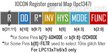
IOCON register for other LPC13x7 devices
For devices like LPC1347 ICOCON register given additional control like:
- Logic Inversion of input pins, if available
- Input Glitch filter, on pins which support it, if available
The general register map for similar devices is as given below:

The different in structure is that:
- Bit 6 now represents INV which is used to invert the Input(HIGH is read LOW and vice-versa) by setting this bit to 1. If the bit is 0 inputs are not inverted.
- For a few pins Bit 8 represents FILTR which is used to enabled/disable glitch filter. 0 means glitch filter is enabled and 1 means its disabled.
Using IOCON registers in programming
In the device header files based on CMSIS viz. lpc11xx.h and lpc13xx.h all the IOCON registers are grouped under LPC_IOCON structure. While programming in C/C++ , these can be accessed as: LPC_IOCON->[register-name]. Where [register-name] is the name of the IOCON register for a specific PIN as given in datasheet/manual.
For example, to access IOCON for PIO0_1(P0.1) in your code you must use LPC_IOCON->PIO0_1 = value.
Eg.:
/*LPC11xx*/
LPC_IOCON->RESET_PIO0_0
LPC_IOCON->PIO0_8
LPC_IOCON->R_PIO0_11
...

/*LPC13xx*/
LPC_IOCON->PIO0_1
LPC_IOCON->SWDIOCLK_PIO0_10
LPC_IOCON->R_PIO1_10
...
