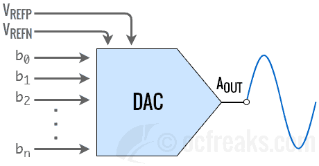
In this article, we will go through a discussion on ARM Cortex-M3 LPC1768 DAC programming tutorial. As you might be knowing, DAC stands for Digital to Analog Conversion. The DAC block in ARM Cortex-M3 LPC176x microcontroller is one of the simplest to program and also supports DMA. This tutorial is also applicable for LPC1769 MCU. Basically we assign a digital value to a register and the DAC block outputs it equivalent analog signal as shown below:

LPC1768/LPC1769 DAC Block
ARM Cortex-M3 LPC176x MCUs incorporate a 10 bit DAC and provide buffered analog output. As per the datasheet, it is implemented as a string DAC which is the most simplest form of DAC consisting of 2N resistors in series where N = no. of bits which simply forms a Kelvin-Varley Divider. LPC176x DAC has only 1 output pin, referred to as AOUT. The Analog voltage at the output of this pin is given as:
+ VREFN
When we have VREFN = 0, the equation boils down to:
Where VALUE is the 10-bit digital value which is to be converted into its Analog counterpart and VREF is the input reference voltage.
Pins relating to LPC1768 DAC block:
| Pin | Description |
|---|---|
| AOUT (P0.26) | Analog Output pin. Provides the converted Analog signal which is referenced to VSSA i.e. the Analog GND. Set Bits[21:20] in PINSEL1 register to [10] to enable this function. |
| VREFP, VREFN | These are reference voltage input pins used for both ADC and DAC. VREFP is positive reference voltage and VREFN is negative reference voltage pin. In example shown below we will use VREFN=0V(GND). |
| VDDA, VSSA | VDDA is Analog Power pin and VSSA is Ground pin used to power the ADC module. These are generally same as VCC and GND but with additional filtering to reduce noise. |
DAC Registers in ARM Cortex-M3 LPC176x
The DAC module in ARM LPC1768/LPC1769 has 3 registers viz. DACR, DACCTRL, DACCNTVAL. In this tutorial we will only go through to DACR register since the other two are related with DMA operation, explaining which is not in the scope of this tutorial. Just note that DMA is used to update new values to DACR from memory without the intervention of CPU. This is particularly useful when generation different types of waveforms using DAC. We will cover this in another tutorial.
Also note that the DAC doesn’t have a power control it in PCONP register. Simply select the AOUT alternate function for pin P0.26 using PINSEL1 register to enable DAC ouput.
The DACR register in LPC1768
The field containing bits [15:6] is used to feed a digital value which needs to be converted and bit 16 is used to select settling time. The bit significance is as shown below:
- Bit[5:0]: Reserved.
- Bit[15:6] – VALUE: After a new VALUE is written to this field, given settling time selected using BIAS has elapsed, we get the converted Analog voltage at the output. The formula for analog voltage at AOUT pin is as shown above.
- Bit[16] – BIAS: Setting this bit to 0 selects settling time of 1us max with max current consumption of 700uA at max 1Mhz update rate. Setting it to 1 will select settling time of 2.5us but with reduce max current consumption of 300uA at max 400Khz update rate.
- Bits[31:17]: Reserved
ARM Cortex-M3 LPC1768 DAC example
As evident, without using DMA, programming the DAC block is very straight forward. We just need to select AOUT function for P0.26 pin and apply a 10-bit value which needs to be converted into its Analog form. Lets see a basic LPC1768 DAC example. For most development boards VREFP will be connected to VDD/VDDA and VREFP will be connected to VSS/VSSA using some form of noise isolation. In this DAC example, we will be changing the output from 0V to VREFP (using VREFN=0V) and then falling back to 0V in steps of 10ms. This DAC program will basically output a sawtooth waveform. We will be using BIAS = 0 i.e. settling time of 1us. You can connect an Oscilloscope or a Multimeter between P0.26 and GND to check the changing analog output. Since the output is buffered you can drive an LED from AOUT but it won’t glow until it reaches its forward bias voltage of around 1.7 Volts. So, keep this in mind when checking for analog output using an LED. Also, I have used Timer0 for generating delay(Alternatively this can be using DMA Timer itself). You can check my previous LPC1768 timer tutorial.

[Note: VSSA and GND will be common for most development boards.]
C/C++ Source Code:
/*(C) Umang Gajera - www.ocfreaks.com
LPC1768 DAC Example 1 Source Code using KEIL ARM
More Embedded tutorials @ www.ocfreaks.com/cat/embedded/
License : GPL.*/

#include <lpc17xx.h>

void initTimer0(void);
void delayMS(unsigned int milliseconds);

int main(void)
{
	//SystemInit(); //gets called by Startup code before main(), sets CCLK = 100Mhz
	initTimer0();
	LPC_PINCON->PINSEL1 |= (1<<21); //Select AOUT function for P0.26 , bits[21:20] = [10]
	unsigned int value=0; //Binary value used for Digital To Analog Conversion
	while(1)
	{
		if(value > 1023) value=0; //For 10-bit DAC max-value is 2^10 - 1 = 1023
		LPC_DAC->DACR = (value<<6);
		delayMS(10);
		value++;
	}
}

void initTimer0(void)
{
	//Refer: http://www.ocfreaks.com/lpc1768-timer-programming-tutorial/
	//Assuming that PLL0 has been setup with CCLK = 60Mhz
	//using default PCLK = 25 which is configure by startup code
	LPC_TIM0->CTCR = 0x0;
	LPC_TIM0->PR = 25000-1; //25000 clock cycles @25Mhz PCLK = 1 ms
	LPC_TIM0->TCR = 0x02; //Reset Timer
}

void delayMS(unsigned int milliseconds) //Using Timer0
{
	LPC_TIM0->TCR = 0x02; //Reset Timer
	LPC_TIM0->TCR = 0x01; //Enable timer
	while(LPC_TIM0->TC < milliseconds); //wait until timer counter reaches the desired delay
	LPC_TIM0->TCR = 0x00; //Disable timer
}
